SMD Transistor PCB
Quality through-hole JFETs are becoming difficult to source, making SMD replacements the best alternative. This PCB is designed to accommodate JFET SMD transistors, allowing you to easily substitute them for traditional through-hole parts.Steps
Categories
Status: Active

SMD Transistor PCB Step 1 of 1
Quality through-hole JFETs are becoming difficult to source, making SMD replacements the best alternative. This PCB is designed to accommodate JFET SMD transistors, allowing you to easily substitute them for traditional through-hole parts.
PCB
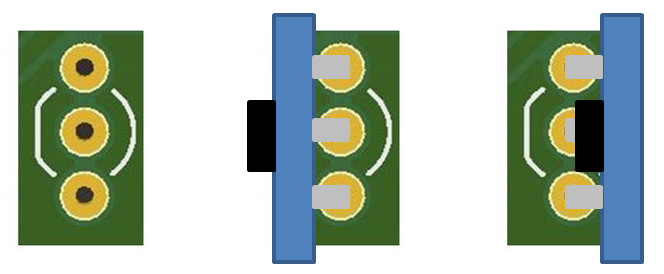
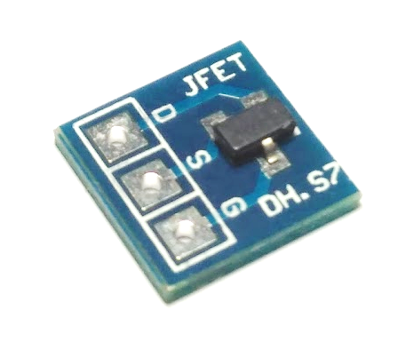
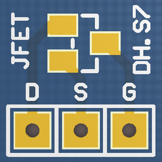
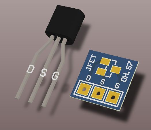
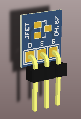
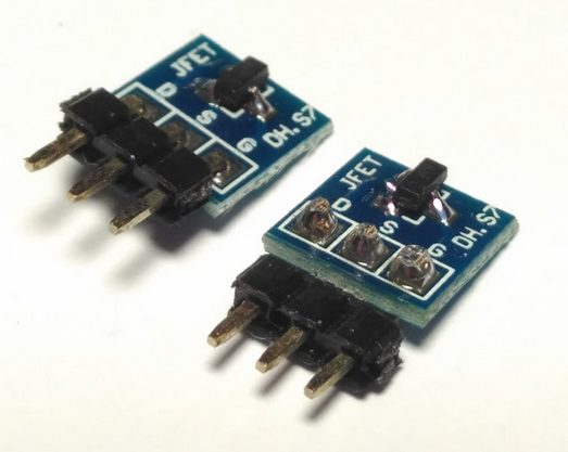
The SMD transistor to TO-92 PCB is marked with the corresponding pads for the Drain (D), Source (S), and Gate (G).
This PCB is designed for transistors like the J201, 2N5457, 2N5458, and MPF102, with the pinout shown in the following figure. If you are using a different type of transistor, please check its datasheet for the correct pinout.
ASSEMBLING THE PCB
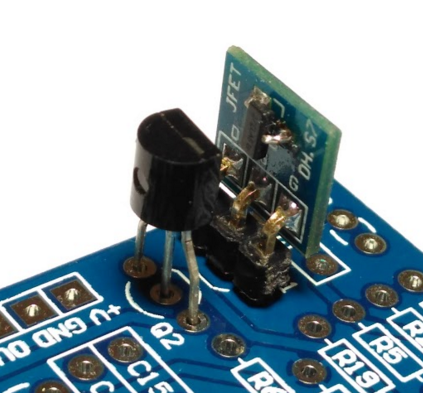
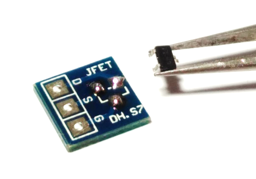
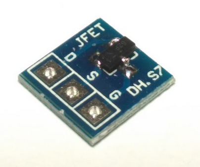
Add a small amount of solder to each pad on the PCB. Using tweezers, carefully place the transistor over the pads. Melt the solder to connect the transistor legs to the PCB pads.
Connect the PCB to the effect circuit using either wires or 2.54 mm right angle headers. The headers can be mounted on either side of the PCB, depending on the space available around the transistor in the effect circuit.
Once the transistor and pin headers are mounted, the PCB can be installed directly onto the original through-hole footprint.